Vadodara
08048037269
+916352984027

pcb assembly and turnkey manufacturing

6814772a5d263414004dd4a4 Card 2

product image
PCB assembly and Turnkey manufacturing

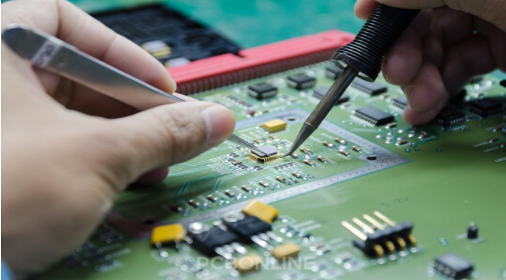
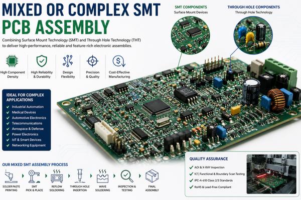
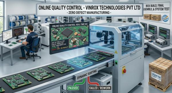
Online Quality Control (OQC) is a systematic process of monitoring, inspecting, and verifying product quality during the manufacturing process. Unlike final inspection alone, OQC ensures that quality checks are performed continuously at every critical production stage, enabling immediate detection and correction of defects before products move to the next operation. In electronics manufacturing, OQC plays a vital role in maintaining product consistency, reducing rework, minimizing production losses, and ensuring customer satisfaction. Online Quality Control refers to real-time inspection and monitoring activities conducted throughout the manufacturing process. By integrating quality checkpoints directly into production lines, manufacturers can identify deviations, defects, and process variations early, ensuring that only products meeting quality standards proceed further. OQC combines visual inspection, automated testing, process monitoring, and statistical analysis to maintain consistent production quality.

6814772a5d263414004dd4a4 Card 2

product image
PCB assembly and Turnkey manufacturing

Board Level Testing and System Level Testing are critical quality assurance processes used to verify the functionality, performance, reliability, and safety of electronic assemblies and finished products. These testing methods help identify defects early, reduce field failures, and ensure that products meet design specifications and industry standards. By implementing comprehensive testing procedures, manufacturers can improve product quality, enhance customer satisfaction, and reduce warranty and maintenance costs. Why Choose Our Board Level and System Level Testing Services? 1. Advanced Testing Infrastructure 2. Experienced Test Engineers 3. Comprehensive Inspection and Validation 4. Customized Test Solutions 5. Reduced Manufacturing Risks 6. Improved Product Reliability 7. Fast Turnaround Times 8. Compliance with Industry Standards

6814772a5d263414004dd4a4 Card 2

product image
PCB assembly and Turnkey manufacturing

Wire and Cable Harnessing is the process of organizing, bundling, and integrating multiple wires, cables, connectors, terminals, and protective coverings into a single assembly. These harnesses simplify electrical installations, improve system reliability, and ensure efficient power and signal transmission across electronic and electrical systems. Cable harness assemblies are widely used in automotive, industrial automation, aerospace, telecommunications, medical equipment, consumer electronics, and renewable energy applications. What is Wire and Cable Harnessing? A wire harness or cable assembly is a structured arrangement of electrical wires and cables designed to transmit power, data, or signals between different components within a system. By grouping and protecting wires in a unified assembly, harnessing improves safety, reduces installation time, and enhances overall system performance. Wire and cable harnesses are custom-designed according to application-specific requirements, ensuring precise connectivity and long-term reliability.

6814772a5d263414004dd4a4 Card 2

product image
PCB assembly and Turnkey manufacturing

Turnkey Manufacturing is a comprehensive production solution where a single manufacturing partner manages the entire product lifecycle—from sourcing components and PCB fabrication to assembly, testing, packaging, and final delivery. This approach simplifies the manufacturing process, reduces operational complexity, and enables businesses to focus on product development, innovation, and market growth. Turnkey manufacturing is widely used across industries such as electronics, medical devices, industrial automation, telecommunications, automotive, aerospace, and consumer products. Turnkey Manufacturing refers to a fully managed production model in which the manufacturer takes responsibility for all aspects of the manufacturing process. Customers provide product specifications, design files, or engineering requirements, and the manufacturing partner handles everything necessary to deliver a finished, ready-to-use product. This integrated approach eliminates the need to coordinate multiple suppliers, vendors, and production facilities.

6814772a5d263414004dd4a4 Card 2

product image
PCB assembly and Turnkey manufacturing

Box Build Assembly, also known as Final Assembly or System Integration, is the process of assembling all electronic and mechanical components into a complete, fully functional product ready for deployment or shipment. It goes beyond PCB assembly by integrating enclosures, wiring, cables, displays, power supplies, connectors, and other subassemblies into a finished system. Box Build services provide a streamlined manufacturing solution, enabling businesses to reduce supply chain complexity, improve product quality, and accelerate time-to-market. Box Build Assembly involves the complete integration of electronic assemblies into an enclosure or finished product housing. The process includes mechanical assembly, cable harness installation, PCB mounting, system wiring, testing, labeling, packaging, and final quality verification. The result is a fully assembled and tested product delivered to the customer ready for installation or end-user operation.

6814772a5d263414004dd4a4 Card 2

product image
PCB assembly and Turnkey manufacturing

Rapid prototyping is the process of quickly designing, manufacturing, and testing electronic prototypes to validate functionality, performance, and manufacturability before full-scale production. It enables engineering teams to identify issues early, reduce development risk, and bring products to market faster. Rapid prototyping is ideal for startups, R&D teams, and product developers working on consumer electronics, industrial automation, medical devices, IoT products, automotive electronics, telecommunications equipment, and aerospace systems.

6814772a5d263414004dd4a4 Card 2

product image
PCB assembly and Turnkey manufacturing

Conformal Coating and Epoxy Potting are specialized protection processes used to enhance the durability, reliability, and lifespan of electronic assemblies. These protective solutions safeguard printed circuit boards (PCBs) and electronic components from moisture, dust, chemicals, vibration, corrosion, and harsh environmental conditions. Widely used across industries such as automotive, aerospace, medical, industrial automation, telecommunications, and defense, these protective processes help ensure consistent performance in demanding operating environments. What is Conformal Coating? Conformal Coating is a thin protective polymer layer applied directly to the surface of a PCB and its components. The coating conforms to the shape of the board and creates a protective barrier against environmental contaminants while maintaining electrical functionality. What is Epoxy Potting? Epoxy Potting is the process of completely encapsulating electronic components or PCB assemblies within a protective resin compound. The epoxy material hardens around the electronics, providing exceptional mechanical strength and environmental protection. Potting is commonly used in applications where electronics must withstand extreme conditions, mechanical stress, or exposure to chemicals and moisture.

6814772a5d263414004dd4a4 Card 2

product image
PCB assembly and Turnkey manufacturing

Through Hole to Surface Mount Technology (SMT) Conversion is the process of redesigning and optimizing existing through-hole printed circuit board (PCB) assemblies to utilize surface mount components. This conversion helps manufacturers improve product performance, reduce manufacturing costs, increase component density, and support modern electronic design requirements. As electronic devices continue to become smaller, faster, and more efficient, SMT conversion has become a strategic solution for upgrading legacy products and extending their market life. Through Hole to SMT Conversion involves replacing traditional through-hole components with equivalent surface mount devices (SMDs) while maintaining the original functionality and performance of the circuit.

6814772a5d263414004dd4a4 Card 2

product image
PCB assembly and Turnkey manufacturing

High-Mix and Low-Medium Volume PCB Assembly is a specialized manufacturing approach designed for businesses that require multiple product variations in smaller production quantities. This assembly model is ideal for prototype development, new product introductions (NPI), customized electronic devices, and specialized industrial applications where flexibility, quality, and rapid turnaround are essential. By combining advanced manufacturing processes with efficient production planning, high-mix assembly enables manufacturers to produce a wide range of PCB designs while maintaining consistent quality and cost efficiency. High-Mix PCB Assembly refers to the production of numerous PCB designs, configurations, or product variants within a manufacturing environment. Each assembly may have different component requirements, specifications, and testing procedures. This manufacturing model is commonly used when product customization and design diversity are more important than high-volume production.

6814772a5d263414004dd4a4 Card 2

product image
PCB assembly and Turnkey manufacturing

Fine Pitch PCB Assembly involves the placement and soldering of ultra-miniature Surface Mount Devices (SMDs), including 0201 and 01005 package components, onto printed circuit boards. These tiny components enable the development of highly compact, lightweight, and high-performance electronic products used in today's advanced technology applications. With increasing demand for miniaturized electronics, fine pitch assembly has become essential for industries requiring high-density circuit designs, superior functionality, and maximum space utilization.

6814772a5d263414004dd4a4 Card 2

product image
PCB assembly and Turnkey manufacturing

Thick Film and Thin Film technologies are advanced manufacturing processes used to create electronic circuits, resistors, sensors, and hybrid microelectronic components. These technologies involve depositing conductive, resistive, or dielectric materials onto a substrate to form highly reliable electronic circuits for various industrial and commercial applications. Both technologies play a critical role in modern electronics, including automotive systems, telecommunications, medical devices, aerospace equipment, industrial automation, and consumer electronics. What is Thick Film Technology? Thick Film Technology involves depositing conductive, resistive, and insulating pastes onto a ceramic or other substrate through a screen-printing process. The printed layers are then fired at high temperatures to create durable and reliable circuit patterns. The thickness of the deposited layer typically ranges from 10 to 100 micrometers, making it significantly thicker than thin film coatings. What is Thin Film Technology? Thin Film Technology involves depositing extremely thin layers of conductive or resistive materials onto a substrate using vacuum deposition techniques such as sputtering, evaporation, or chemical vapor deposition (CVD). The deposited layers typically range from nanometers to a few micrometers in thickness, allowing highly precise electrical characteristics and superior circuit performance.

6814772a5d263414004dd4a4 Card 2

product image
PCB assembly and Turnkey manufacturing

Mixed or Complex SMT PCB Assembly combines Surface Mount Technology (SMT) and Through Hole Technology (THT) on a single Printed Circuit Board (PCB). This advanced assembly process is designed for sophisticated electronic products that require both high-density surface-mounted components and mechanically robust through-hole components. Complex SMT assembly is widely used in industries where reliability, performance, and intricate circuit designs are essential. It enables manufacturers to create compact, multifunctional, and high-performance electronic systems. Mixed Technology PCB Assembly involves integrating Surface Mount Devices (SMDs) and Through Hole Components (THCs) onto the same PCB. The assembly process typically includes solder paste printing, automated pick-and-place component placement, reflow soldering, manual or automated through-hole insertion, wave soldering, and comprehensive testing.

Subcategory Tags

Phone Number

08048037269

Please keep 0 before dialling the number.

Email Address sales@vinrox.com

Mon-Thu: 10 AM - 2 PM • Fri: 3 PM - 7AM

Address 336/22 , Makarpura GIDC , Makarpura

Vadodara, India, 390010