
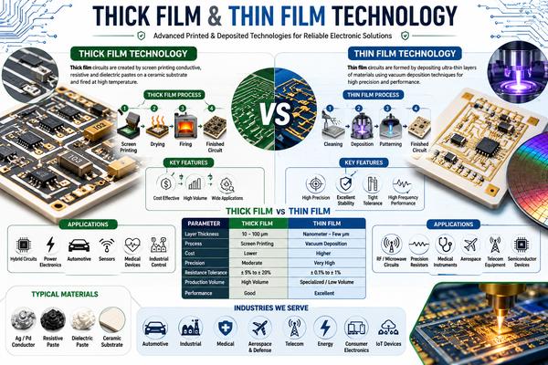
Thick Film and Thin Film technologies are advanced manufacturing processes used to create electronic circuits, resistors, sensors, and hybrid microelectronic components. These technologies involve depositing conductive, resistive, or dielectric materials onto a substrate to form highly reliable electronic circuits for various industrial and commercial applications. Both technologies play a critical role in modern electronics, including automotive systems, telecommunications, medical devices, aerospace equipment, industrial automation, and consumer electronics. What is Thick Film Technology? Thick Film Technology involves depositing conductive, resistive, and insulating pastes onto a ceramic or other substrate through a screen-printing process. The printed layers are then fired at high temperatures to create durable and reliable circuit patterns. The thickness of the deposited layer typically ranges from 10 to 100 micrometers, making it significantly thicker than thin film coatings. What is Thin Film Technology? Thin Film Technology involves depositing extremely thin layers of conductive or resistive materials onto a substrate using vacuum deposition techniques such as sputtering, evaporation, or chemical vapor deposition (CVD). The deposited layers typically range from nanometers to a few micrometers in thickness, allowing highly precise electrical characteristics and superior circuit performance.